Analysis of semiconductors
from raw material to finished IC
A semiconductor is a solid whose electrical conductivity varies between that of insulators and conductors, depending on the temperature. Typical semiconductors are based on the elements silicon or germanium. But compounds such as gallium arsenide or indium phosphide (III-V semiconductors) and some organic materials also have semiconducting properties. The characteristics of a semiconductor can be changed both through the choice of the semiconductor material and through targeted modifications (doping, implantation). In combination with sophisticated structuring methods (lithography, deposition of insulator layers, etching processes, ...) electronic components (e.g. diodes, transistors) are created that are used in almost all electronic devices such as computers, cars, solar modules or flashlights.
The performance and service life of semiconductor components depend heavily on the purity of the used raw materials and the precision of the many individual process steps involved in manufacturing. For this reason, the production of semiconductors is closely monitored by various analytical techniques to ensure quality. At the same time, these techniques play an important role in the development of ever smaller semiconductor structures and for error analysis.
In the Tascon laboratory, the analysis of semiconductors has been part of our range of tasks for more than 20 years. For these analyses, we use surface analytical methods such as SEM/EDX, ToF-SIMS, XPS or LEIS to provide answers to the various questions. The following list gives you an overview of typical analyses that we carry out for our customers.
Analysis of high purity semiconductor materials
Determination of the chemical bulk composition of a semiconductor
Ultrapure silicon wafers are manufactured from single crystal rods in a multi-step process. Depending on the later application, dopants can be added when the single crystals are pulled. On the other hand, unintentional contamination (trace impurities) such as carbon or foreign metals is undesirable. For this reason, many semiconductor manufacturers use analysis techniques such as ToF-SIMS or ICP-OES (MS) to quantitatively examine the chemical composition of freshly manufactured wafers. These methods are also used in the analysis of III-V semiconductors. However, these III-V semiconductor analyses are often not only about doping and trace impurities, but also about the mixing ratio of the matrix elements. The depth profile in the left part of figure 1a shows an example of such an analysis on a SiGe multilayer system that illustrates the possibilities of quantification with the ToF-SIMS method.
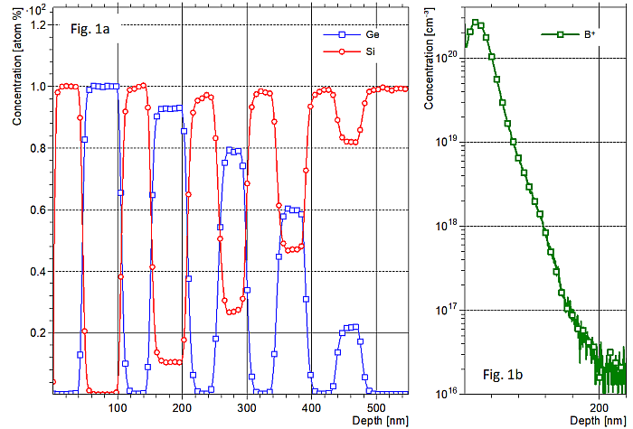
In addition to the characterization of semiconductor materials, (partially) processed semiconductor structures are also regularly examined in our laboratories. Typical questions are, for example, the changes in regions close to the surface due to temperature-driven migration and diffusion processes or the control of implantation profiles that are used to specifically change the electrical properties of the semiconductor material. Such a profile of boron in silicon is shown in Figure 1b.
Analysis of the surface of a semiconductor
Even if the volume of a semiconductor shows no chemical abnormalities, the surface of a semiconductor may very well be contaminated. Impurities can be in the form of particles or as thin film impurities.
These days, particle contamination is minimized as much as possible with the use of the latest clean room technology during production. If, despite this, particles appear, scanning electron microscopy (SEM-EDX) in Tascon's laboratory is usually 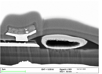 the first choice for the investigation of the cause. With these cleanliness analyses, particles are localized, the particle topography is determined and the elementary composition of the particles is determined. Should the SEM / EDX provide information on organic contamination, ToF-SIMS analyzes can provide information on the organic composition of the examined particles.
The ToF-SIMS method is also very suitable for analyzing film contamination. Film contamination often consists of process residues (e.g. photoresist, surfactants), adsorbates from the clean room air (e.g. plasticizers, fats) or contamination from tools and can be sensitively detected and identified with ToF-SIMS. At the same time, the method also records elementary residues, so that inorganic residues (e.g. abrasives from a polish, salts) can be detected too.
Analysis of extremely thin layers
Quantification of the composition, layer thickness and cohesion
Due to the advancing miniaturization of integrated circuits, the semiconductor industry is increasingly interested in extremely thin metallic or insulating layers.
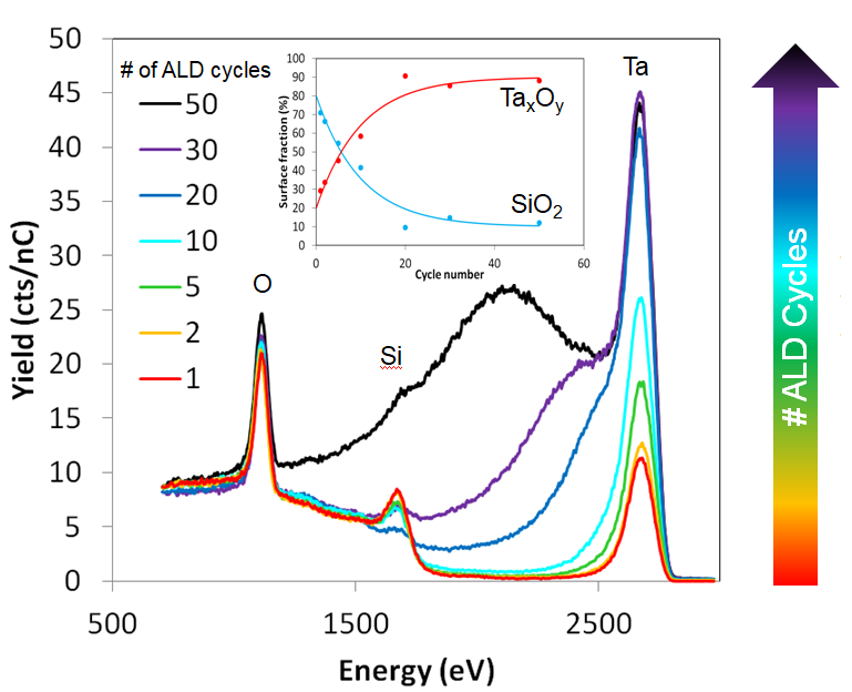
In our laboratory, the characterization of extremely thin layers, e.g. manufactured by Atomic Layer Deposition (ALD) is carried out primarily with Low Energy Ion Scattering (LEIS). LEIS is a method that enables quantitative element analyses of the outermost atomic layer and thus allows the investigation of growth processes and the determination of layer closeness and average layer thicknesses. The example shown here of ALD tantalum oxide layers on Silicon oxide was used to optimize the ALD process and to determine the number of ALD cycles required until the layer is closed.
Further details on similar analyzes of ALD films can be found here.
Analysis of unknown layer structures and detection of contamination at interfaces and localized defects
Semiconductor structures often consist of a large number of consecutive individual layers and complex structures. If abnormalities are observed during electrical or spectroscopic tests, the question arises as to where in the complex three-dimensional layer system the cause could be found. The number of possible errors is very large, so that ideally an analysis technique is used for characterization that enables an examination of the complete layer structure and a sensitive detection of all elements in one analysis step. Modern ToF-SIMS instruments offer these possibilities. In many cases it is possible to characterize these complex multi-layer systems without any problems so that possible errors can be identified. In this way, typical questions about contamination or oxidation at interfaces, foreign metals in layers, intermixing of layers, layer thickness variations or buried defects can be answered quickly. A typical example of such an analysis of a metallic coating for an optical application can be found here.
But similar cases are also held responsible for failures in the field of organic semiconductors. Analogous to the inorganic systems, impurities, intermixing, thickness variations or defects in layers or oxidative decay of molecules can be observed in organic semiconductors, which can be examined more precisely using organic ToF-SIMS depth profiles or high-resolution hybrid SIMS analyses.
Analysis of bond pads and bonding errors
The dice (semiconductor wafer pieces with the complete integrated circuit) are connected using thin wires at so-called bond pads (see SEM picture). During wire bonding, various types of defects (e.g. detachment of the bonding surface due to a defective layer structure, lifting of the bonding wire, discoloration of the bond pad or corrosion, ...) can be observed, the cause of which can be determined by suitable analyses depending on the exact defect pattern. An example of an XPS analysis of a discolored bond pad surface can be found here.
Other typical semiconductor issues
In addition to the analyses of semiconductor materials presented here in more detail, we repeatedly receive questions on the following topics:
- Analysis of implantation profiles
- Migration of metals (e.g. dendrite formation from Cu)
- Embrittlement of materials
- Diffusion processes in semiconductor layers
- Packaging: Defects in casting or corrosion protection coating of semiconductors and circuit boards
- Clarification of unknown semiconductor layer structures to protect own patents (reverse engineering)
- Basic research on the diffusion of semiconductor materials
Tascon - your laboratory for the analysis of semiconductors
If your question cannot be found among the examples of typical semiconductor analyzes at Tascon described above, please do not hesitate to contact us. In a non-binding consultation, we determine your individual needs for analytics and offer you a tailor-made analytical solution to your question.
Get in touch. Contact one of our analytical professionals:
(845)-352-1220